Designing for Success : Tips and Tricks for Optimal HDI PCB Layouts delves into the intricacies of high-density interconnect boards. The emphasis lies on the preservation of signal integrity, a facet of paramount significance to achieve superior functionality. The discourse then shifts to the realm of advanced material choices, highlighting their instrumental role in fortifying the reliability of HDI PCBs. A detailed examination of various materials and their impact on performance and durability ensues, providing fresh insights into the art of HDI PCB design. Finally, the spotlight is turned onto thermal management techniques, revealing their indispensable role in ensuring efficient high-speed layouts. This diverse discussion promises to be an enlightening journey through the labyrinth of HDI PCB layout design.
Ensuring signal integrity in high-density interconnect boards
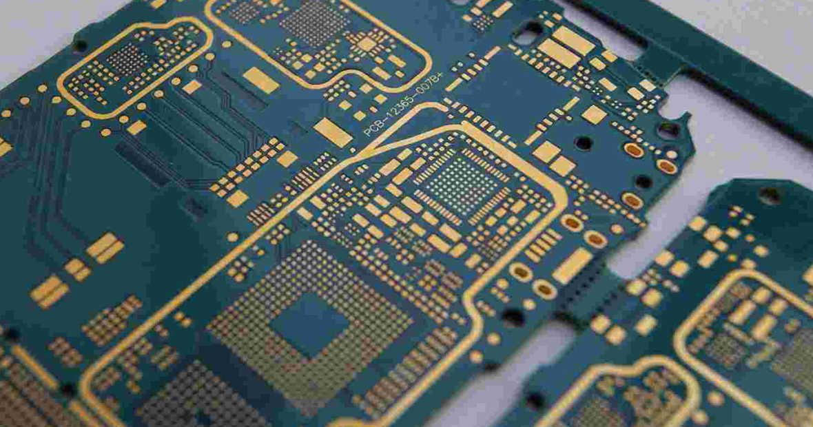
Within the realm of high-density interconnect (HDI) PCB layouts, maintaining signal integrity proves paramount. This realm requires a comprehensive understanding of the challenges and techniques used to uphold signal integrity. One must grasp the impact of the non-adherence to signal integrity on the performance and reliability of high-density interconnect boards. A prime example of a solution to these challenges can be found on icape-group.com, where they utilize the latest technologies and innovations in their designs to ensure signal integrity.
Signal integrity remains critical in modern high-density applications. High-density interconnect (HDI) PCBs rely heavily on signal integrity for optimal performance. To minimize signal integrity issues, careful consideration must be given to the routing of traces and the placement of vias and microvias during the layout design. Many common errors encountered during the design of high-density interconnect boards can be avoided with the appropriate knowledge and skills. Software tools are available to aid in the design and analysis of signal integrity in these boards. The choice of materials and fabrication techniques also has a profound effect on signal integrity. Case studies illustrate the importance and methods of ensuring signal integrity in these boards. Expert recommendations provide best practices for maintaining signal integrity in these high-density interconnect boards. It is essential for those in the field to continuously update their skills to understand and manage signal integrity in these complex devices. Anticipated future trends in high-density interconnect board design and signal integrity continue to evolve, further emphasizing the importance of ongoing education and skill development.
Advanced material choices for enhanced hdi pcb reliability
Reliability and performance of High Density Interconnect (HDI) Printed Circuit Boards (PCBs) largely depend on the strategic selection of advanced materials. One of the most significant factors enhancing the reliability of HDI PCBs is the use of materials with a low coefficient of thermal expansion. This ensures the stability of the board in fluctuating temperature environments, enhancing the overall reliability of the device.
Exploring Advanced Material Selection for HDI PCB
Advanced materials play a pivotal role in reducing impedance and improving the electrical performance of HDI PCBs. High conductivity materials offer a superior solution for heat management in HDI PCBs, thereby increasing the efficiency of electronic devices. Precise and reliable assembly of electronic components on HDI PCBs is heavily influenced by the choice of materials.
Improving HDI PCB Reliability with Strategic Material Choices
Material selection criteria are paramount in optimizing the durability and reliability of HDI PCBs against mechanical stresses. The right material choices can enhance the manufacturing process, leading to more reliable and durable boards.
Enhancing Performance and Durability of HDI PCBs through Superior Material Selection
Eco-responsible material choices for HDI PCB design contribute to the development of more sustainable and environmentally friendly electronics. By following the correct guidelines and rules, designers can leverage advanced technology to create PCBs that meet high standards of reliability and performance.
Thermal management techniques in high-speed hdi pcb layouts
High-speed HDI PCB layouts present unique challenges, one of which is thermal management. Ensuring optimal heat dissipation is paramount for the durability and performance of these densely packed circuit boards. Different thermal management techniques exist for HDI PCBs, each with their unique advantages and disadvantages. These techniques are vital in maintaining the speed of HDI PCB designs.
Components and traces on the board must be arranged thoughtfully to allow for efficient heat distribution. Mismanagement of thermal aspects often leads to poor performance and can even damage the assembly. Materials used in the design process play a significant role in heat management. For instance, high-speed HDI PCB designers often need to consider the use of specific materials known for their heat minimization properties.
Signal routing in the PCB layout is another crucial aspect that contributes to efficient thermal management. To maintain the required impedance level, electronic designers must keep signal paths short and direct. This process involves careful placement of vias and microvias, which help distribute heat across different layers of the board and thus prevent potential heat issues.
Recent technological advancements have brought forth various software tools that aid in thermal management of HDI PCB designs. These tools help designers read and interpret thermal data, thereby enabling them to make informed decisions during the design process. Flex PCBs, due to their adaptability, are being increasingly incorporated into high-speed layouts for improved heat management and enhanced overall performance.
Effective thermal management is a key contributor to the energy efficiency of HDI PCBs. Future developments in this field are expected to further enhance the performance and longevity of these complex electronic assemblies. Therefore, understanding and implementing optimal thermal management techniques is critical for the success of any high-speed HDI PCB layout.